暑期实习准备——Verilog手撕代码(持续更新中。。。
暑期实习准备——手撕代码
- 牛客刷题笔记
- Verilog快速入门
- VL4 移位运算与乘法
- VL5 位拆分与运算
- VL6 多功能数据处理器
- VL8 使用generate…for语句简化代码
- VL9 使用子模块实现三输入数的大小比较
- VL11 4位数值比较器电路
- VL12 4bit超前进位加法器电路
- VL13 优先编码器电路①
- VL14 用优先编码器①实现键盘编码电路
- VL16 使用8线-3线优先编码器Ⅰ实现16线-4线优先编码器
- VL17 用3-8译码器实现全减器
- VL19 使用3-8译码器①实现逻辑函数
- VL20 数据选择器实现逻辑电路
- VL21 根据状态转移表实现时序电路
- VL22 根据状态转移图实现时序电路
- VL23 ROM的简单实现
- VL24 边沿检测
- Verilog进阶挑战
- Verilog企业真题
- VL25 输入序列连续的序列检测
- VL38 自动贩售机1
- 常见数字IC手撕代码
牛客刷题笔记
牛客Verilog题库
Verilog快速入门
VL4 移位运算与乘法
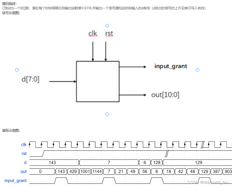
- 要点1:题目用状态机实现,经典的三段式模板。
- 要点2:需要一个d_reg信号临时记录当前要加倍的d信号,这样才能保证d信号变化时,加倍的仍然是原本的d信号,注意d_reg<=d;赋值语句的位置。第3段时钟上升沿触发输出信号的变化,注意
d_reg<=d;赋值语句需要写作阻塞赋值语句的形式,即先完成赋值操作,才能够输出out<=d_reg;。 - 要点3:注意第2、3段敏感事件表的编写,分清什么信号会触发什么操作。
- 要点4:注意为状态机以及其他输出信号赋初始值。
- 要点5:1、3、7、8倍数通过移位运算和加运算实现,不需要乘法运算。
`timescale 1ns/1ns
module multi_sel(
input [7:0]d ,
input clk,
input rst,
output reg input_grant,
output reg [10:0]out
);
//*************code***********//
reg[1:0] current_state,next_state;
reg[7:0] d_reg;always @ (posedge clk or negedge rst) beginif(!rst) current_state<=2'b00;else current_state<=next_state;
endalways @ (current_state) beginnext_state<=2'b00;case(current_state)2'b00:next_state<=2'b01;2'b01:next_state<=2'b10;2'b10:next_state<=2'b11;2'b11:next_state<=2'b00;endcase
endalways @ (posedge clk or negedge rst) beginif(!rst) begininput_grant<=0;out<=0;d_reg<=d;endelse begincase(current_state)2'b00:begin input_grant<=1'b1;d_reg=d;out<=d_reg;end2'b01:begin input_grant<=1'b0;out<= d_reg + {2'b0, d_reg, 1'b0};end2'b10:begin input_grant<=1'b0;out<=d_reg + {2'b00, d_reg, 1'b0} + {1'b0 ,d_reg, 2'b00};end2'b11:begin input_grant<=1'b0;out<={d_reg, 3'b000};endendcaseend
end//*************code***********//
endmodule
VL5 位拆分与运算
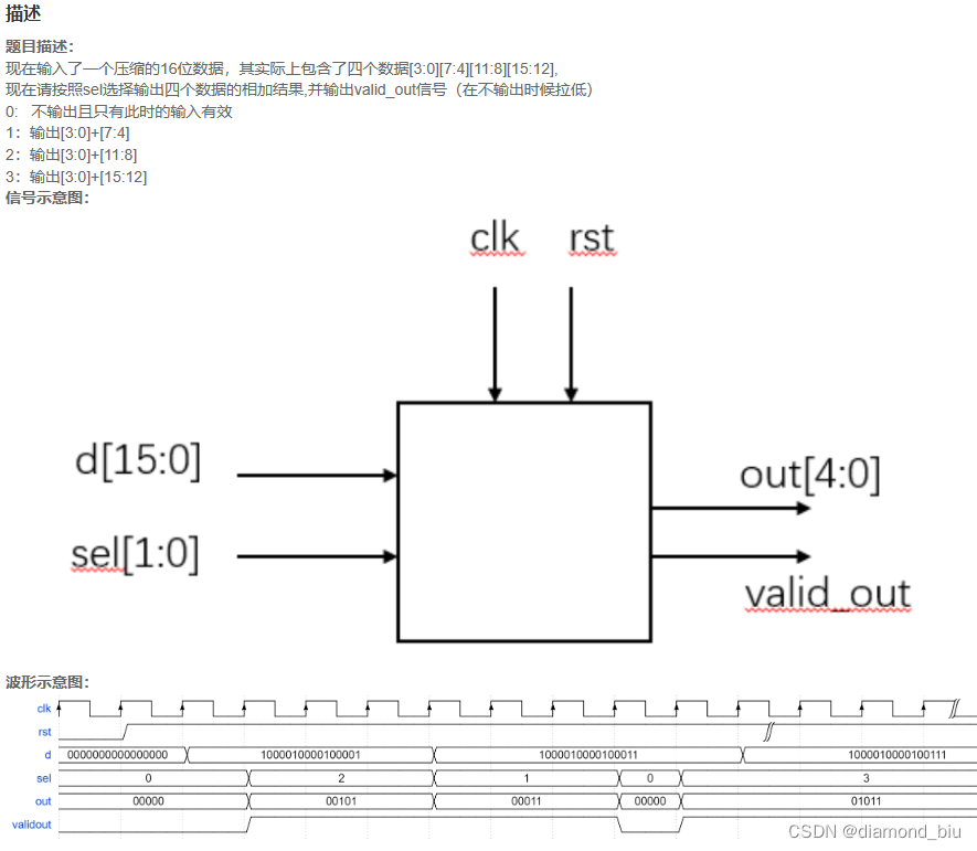
- 要点1:仔细读题,注意题目中提到的只有在sel=0时输入才有效,因此需要reg_d把输入d锁存。
- 要点2:仔细读题,还是要理解题目的意思。
`timescale 1ns/1nsmodule data_cal(
input clk,
input rst,
input [15:0]d,
input [1:0]sel,output reg [4:0]out,
output reg validout
);
//*************code***********//
reg [15:0] reg_d;always @ (posedge clk or rst or d) beginif(!rst) beginout<=5'b0;validout<=0;endelse begincase(sel)2'b00:begin out<=5'b0; validout<=0; reg_d<=d ;end2'b01:begin out<=reg_d[3:0]+reg_d[7:4]; validout<=1; end2'b10:begin out<=reg_d[3:0]+reg_d[11:8]; validout<=1; end2'b11:begin out<=reg_d[3:0]+reg_d[15:12]; validout<=1; endendcaseend
end
//*************code***********//
endmodule
VL6 多功能数据处理器
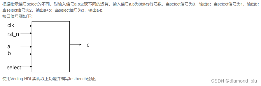
- 要点1:有符号数以补码形式存储,可以直接进行加减运算。
- 要点2:
always @ (posedge clk or negedge rst_n)的写法是正确的,但有点疑惑是初始状态下就是低电平会不会触发,本题既然是正确的就说明初始低电平会触发。
always @ (posedge clk or rst_n)的写法是错误的,会在rst_n由0变为1时触发,但此时可能并非时钟上升沿,造成异常输出。
always @ (posedge clk)的写法会使得初始状态下输出信号处于无效状态,额外在always块前加上initial c<=9'b0;这样可以通过测试用例,但是initial语句不可综合,最好不要使用。
`timescale 1ns/1ns
module data_select(input clk,input rst_n,input signed[7:0]a,input signed[7:0]b,input [1:0]select,output reg signed [8:0]c
);always @ (posedge clk or negedge rst_n) beginif(!rst_n) beginc<=9'b0;endelse begincase(select)2'b00:begin c<=a; end2'b01:begin c<=b; end2'b10:begin c<=a+b; end2'b11:begin c<=a-b; endendcaseend
end
endmodule
VL8 使用generate…for语句简化代码
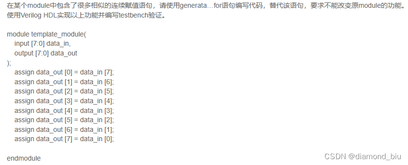
- 要点1:必须使用
genvar声明循环变量。 - 要点2:
begin-end之间插入赋值语句,begin后面必须声明循环实例的名称。 - 要点3:
generate-for常用来简化assign的赋值,assign data_out[i]=data_in[7-i];展开后的8条assign语句是并行赋值的。如,在6线-64线、8线-256线译码器中可以用来简化代码。
`timescale 1ns/1ns
module gen_for_module( input [7:0] data_in,output [7:0] data_out
);genvar i;generate for(i=0;i<=7;i=i+1)begin:labelassign data_out[i]=data_in[7-i];endendgenerate
endmodule
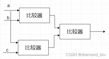
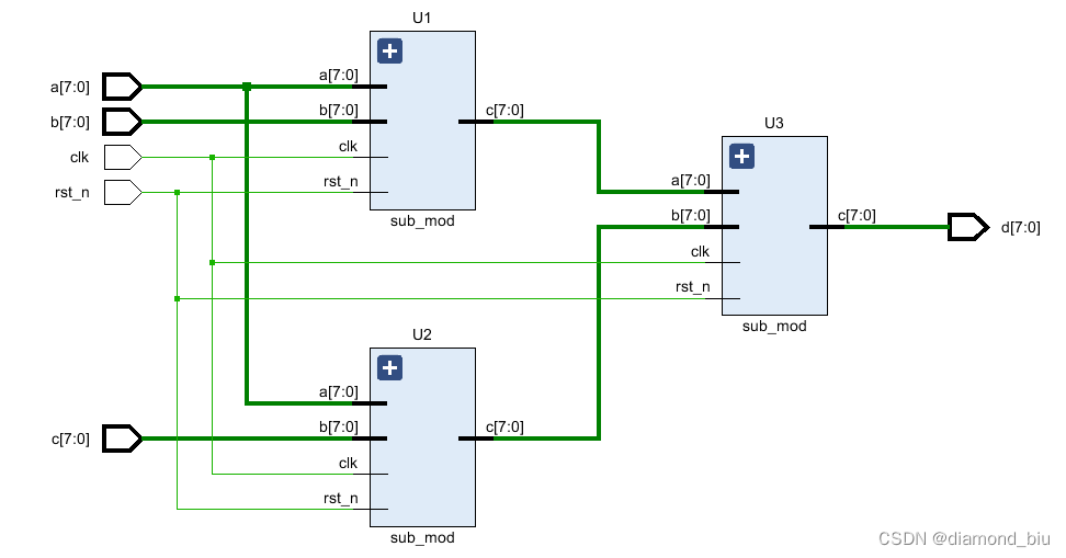
VL9 使用子模块实现三输入数的大小比较
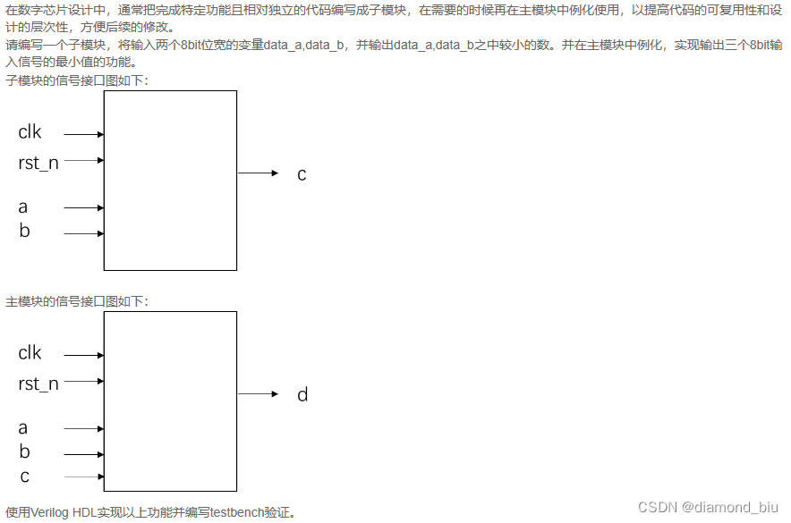
- 要点1:两个比较器会导致进入比较器的三个输入时间不同步,需要使用三个子模块才可以正确实现。
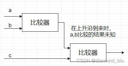
在第一个上升沿,ab进入第一个比较器,c进入第二个比较器。但是比较器输出是需要时间的,在第一个上升沿,c立刻进入第二个比较器,但ab比较器的输出会较晚的进入第二个比较器,这就造成了输入时间不同步,从而造成输出错误。
使用三个比较器将c延迟一拍,就可以让输入子模块的时间都相等,从而不会出现进入时间不同导致的错误。
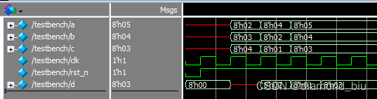
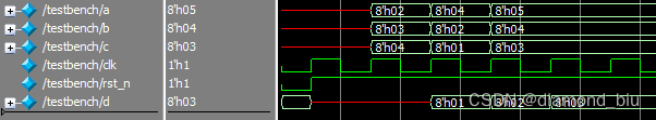
我们可以对波形进行分析来比较这两种写法的差别,testbench如下:
`timescale 1ns/1ns
module testbench();reg signed [7:0] a,b,c;reg clk,rst_n;wire [7:0]d;
main_mod dut(.clk(clk),.rst_n(rst_n),.a(a),.b(b),.c(c),.d(d)
);
always #5 clk = !clk;
initial beginclk=0;rst_n=0;#5 rst_n=1;#10 a=2;b=3;c=4;#10 a=4;b=2;c=1;#10 a=5;b=4;c=3;
end
endmodule
三个比较器的仿真波形如下。可以看到每一次比较的结果都在下一个时钟周期输出,分别为2,1,3。
二个比较器的仿真波形如下,此时比较结果为1,2,3,这是因为上一轮a,b的最小值实际上是与当前周期的c进行比较的,因此对于第一组输入,a和b的比较结果是2,2和下一组输入的c=1进行了比较,所以输出的最小值是1;同样第二组输出,a和b的比较结果是2,2和下一组输入的c=3进行了比较,所以输出为2;第二组输出,a和b的比较结果是4,4和下一组输入的c=3进行了比较,所以输出为3。
- 要点2:子模块中
c<=(a>b)?b:a;语句需要使用非阻塞赋值。
不知道为什么非阻塞不会报错,阻塞会报错显示有用例不通过。使用vivado综合出来的电路这两个是一样的。待解决!!!
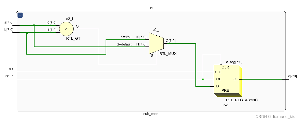
但还是复习一下阻塞赋值和非阻塞赋值
非阻塞赋值b <= a;:非阻塞赋值中赋值并不是马上执行的,也就是说"always"块内的下一条语句执行后,b并不等于a,而是保持原来的值。"always"块结束后,才进行赋值。
阻塞赋值b=a;:方式是马上执行的。也就是说执行下一条语句时,b已等于a。
`timescale 1ns/1ns
module main_mod(input clk,input rst_n,input [7:0]a,input [7:0]b,input [7:0]c,output [7:0]d
);
wire [7:0] ab,ac;
sub_mod U1(.clk(clk),.rst_n(rst_n),.a(a),.b(b),.c(ab));
sub_mod U2(.clk(clk),.rst_n(rst_n),.a(a),.b(c),.c(ac));
sub_mod U3(.clk(clk),.rst_n(rst_n),.a(ab),.b(ac),.c(d));
endmodulemodule sub_mod(clk,rst_n,a,b,c);input clk,rst_n;input[7:0] a,b;output [7:0] c;reg[7:0]c;always@(posedge clk or negedge rst_n)beginif(~rst_n)c<=8'b0;else beginc<=(a>b)?b:a;endend
endmodule
VL11 4位数值比较器电路
要点1:题目中说要用门级描述完成,对于1bit数的比较对应的门运算如下,A>B对应~A&B,A 要点2:抽象描述可以写到直接比较A和B。 加法器与半加器 1比特进位加法器的两种实现: 多位数进位加法器 测试代码: 要点1:题目给的是I1-I9,注意顺序。 要点3:《CPU设计实战》这本书中提到在CPU设计中必须遵守的硬性规定是代码中禁止出现 要点1:编码的结果为 要点1:最小项与最大项。 要点1:熟悉逻辑函数的两种表示形式,最小项和最大项。以本题为例,将逻辑表达式写为最小项形式,即 要点1:牛客的题解写的很清楚了,化简后找对应项要动手推一下。 要点1:根据同步时序电路的设计方法,由状态转换表写出激励方程和输出函数即可。 要点2:也可以采用有向状态机的写法。状态转移图如下: 与VL21类似。 要点2:状态机经典三段式。 要点1:根据题目给出的反例可以看到,在非时钟上升沿,输入的addr改变,输出的data也会改变,因此data=rom_array[addr];这一赋值应该是组合逻辑而非时序逻辑。反例如下: 要点1:参考Verilog设计(四):边沿检测。将原始波形a分别延迟1拍、2拍得到a[0]和a[1],上升沿检测即 要点2:用状态机写,共有3个状态。在 要点3:还是状态机(我的写法,找了两天bug的结果,心累… 要点1:使用优先状态机,经典三段式。 要点2:8bit线性移位寄存器,使用8位寄存器寄存历史序列,并与目标序列比较。 数字IC笔试面试题汇总`timescale 1ns/1nsmodule comparator_4(input [3:0] A ,input [3:0] B ,output wire Y2 , //A>Boutput wire Y1 , //A=Boutput wire Y0 //AB[3])|((A[3]==B[3])&(A[2]>B[2]))|((A[3]==B[3])&(A[2]==B[2])&(A[1]>B[1]))|((A[3]==B[3])&(A[2]==B[2])&(A[1]==B[1])&(A[0]>B[0]));
assign Y1=(A==B);
assign Y0=(A[3]`timescale 1ns/1ns
module comparator_4(input [3:0] A ,input [3:0] B ,output wire Y2 , //A>Boutput wire Y1 , //A=Boutput wire Y0 //AB)?1:0;
assign Y1=(A==B)?1:0;
assign Y0=(AVL12 4bit超前进位加法器电路
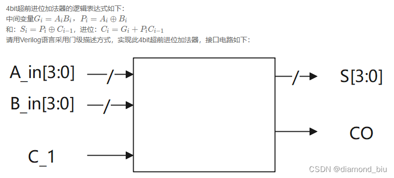
超前进位加法器//实现1:逻辑代数
assign sum=a^b^cin;
assign cout=a&b|(cin&(a^b));或者assign cout=(a&b)|(a&cin)|(b&cin);
//实现2:抽象描述
assign {cout,sum}=a+b+cin;
assign cout=(a&b)|(a&cin)|(b&cin);很容易理解,即a,b,cin中任意两个或以上为1就进位。
assign cout=a&b|(cin&(a^b));可以理解为除了a,b为1的情况外,还有c为1同时 a和b中任意一个为1(a^b)。
多位数进位加法器的实现有两种方式:串行进位加法器、超前进位加法器。
串行进位加法器就是将1比特加法器级联。
超前进位加法器是对串行全加器进行改良设计的并行加法器,以解决普通全加器串联互相进位产生的延迟。
一位全加器的进位的运算逻辑(前面的式子是(A^B)这里是(A|B),对结果没有影响,|包含了^):
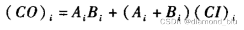
其中,令进位函数Gi = AiBi, 令进位传送函数Pi = Ai + Bi;
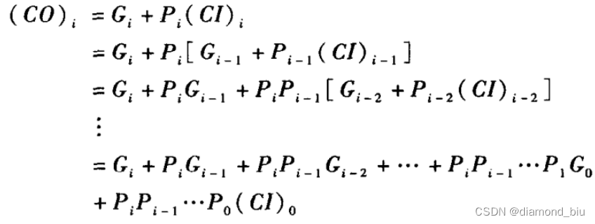
对于4比特超前进位加法器来说,进位输出如下:
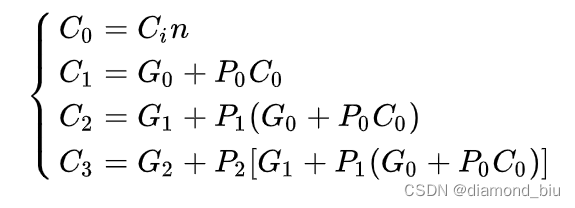
Si=Ai^Bi^(CI)i,对应的(CI)i=(CO)i-1,即Si=Ai^Bi^(CO)i-1。通过前面的推导已经得出了,可得:
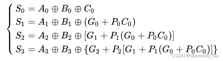
COi=(Ai&Bi)|(CIi&(Ai|Bi))。`timescale 1ns/1nsmodule lca_4(input [3:0] A_in ,input [3:0] B_in ,input C_1 ,output wire CO ,output wire [3:0] S
);
wire[3:0] g,p,c;
assign p=A_in|B_in;
assign g=A_in&B_in;
assign c[0]=g[0]|(p[0]&C_1);
assign c[1]=g[1]|(p[1]&(g[0]|(p[0]&C_1)));
assign c[2]=g[2]|(p[2]&(g[1]|(p[1]&(g[0]|(p[0]&C_1)))));
assign c[3]=g[3]|(p[3]&(g[2]|(p[2]&(g[1]|(p[1]&(g[0]|(p[0]&C_1)))))));
assign CO=c[3];assign S=A_in^B_in^{c[2:0],C_1};
endmodule
`timescale 1ns/1ns
module testbench();
reg[3:0] A_in,B_in;
reg C_1;
wire CO;
wire[3:0] S;
reg[7:0] num;lca_4 U1(.A_in(A_in),.B_in(B_in),.C_1(C_1),.CO(CO),.S(S));
initial beginC_1=0;num=0;
end
always #10 begin num=num+1;A_in<=num[3:0];B_in<=num[7:4];
end
endmodule
VL13 优先编码器电路①
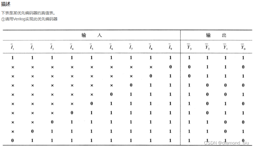
要点2:case、casez和casex三者都是可以综合的。case进行全等匹配,casez忽略?或z对应的位进行匹配,casex忽略x、?或z对应的位进行匹配。`timescale 1ns/1ns
module encoder_0(input [8:0] I_n,output reg [3:0] Y_n
);
always@(I_n)begincasez(I_n)9'b111111111:Y_n<=4'b1111;9'b0????????:Y_n<=4'b0110;9'b10???????:Y_n<=4'b0111;9'b110??????:Y_n<=4'b1000;9'b1110?????:Y_n<=4'b1001;9'b11110????:Y_n<=4'b1010;9'b111110???:Y_n<=4'b1011;9'b1111110??:Y_n<=4'b1100;9'b11111110?:Y_n<=4'b1101;9'b111111110:Y_n<=4'b1110;endcase
end
endmodule
casez、casex,因此可以采用如下写法,看Y9~Y0中出现的第一个0的位置。`timescale 1ns/1ns
module encoder_0(input [8:0] I_n,output [3:0] Y_n
);
assign Y_n=(~I_n[8])?4'b0110:(~I_n[7])?4'b0111:(~I_n[6])?4'b1000:(~I_n[5])?4'b1001:(~I_n[4])?4'b1010:(~I_n[3])?4'b1011:(~I_n[2])?4'b1100:(~I_n[1])?4'b1101:(~I_n[0])?4'b1110:4'b1111;
endmodule
VL14 用优先编码器①实现键盘编码电路

题目描述的不是很清楚。
要点1:GS:按下为1,不按为0,需要注意的是最后assign GS=(S_n==10'b1111111111)?1'b0:1'b1;并不能只判断S_n[0]==1,因为其他按键(9~1)被按下时S_n[0]也为0;
要点2:最终的输出需要对译码结果取反assign L=~Y_n;`timescale 1ns/1nsmodule encoder_0(input [8:0] I_n ,output [3:0] Y_n
);
assign Y_n=(~I_n[8])?4'b0110:(~I_n[7])?4'b0111:(~I_n[6])?4'b1000:(~I_n[5])?4'b1001:(~I_n[4])?4'b1010:(~I_n[3])?4'b1011:(~I_n[2])?4'b1100:(~I_n[1])?4'b1101:(~I_n[0])?4'b1110:4'b1111;
endmodulemodule key_encoder(input [9:0] S_n , output wire[3:0] L ,output wire GS
);wire[3:0] Y_n;encoder_0 U1(.I_n(S_n[9:1]),.Y_n(Y_n));//GS:按下为1,不按为0assign GS=(S_n==10'b1111111111)?1'b0:1'b1;assign L=~Y_n;
endmodule
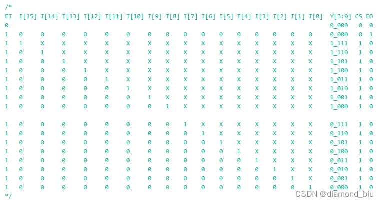
VL16 使用8线-3线优先编码器Ⅰ实现16线-4线优先编码器
000时,可能有三种情况,(1)译码器没有使能,不工作,此时GS=0;EO=0;(2)译码器再工作,但无输入,GS=0;EO=1;;(3)译码器在工作,且有输入,输入为0000_0001,GS=1;EO=0;;
要点2:参考SNx4HC148 8-Line to 3-Line Priority Encoders理解如何使用两个8-3译码器得到一个16-4译码器。实际就是将两个8-3译码器的EO与EI连接,输出取或运算作为译码结果的低3位I[2:0],高位译码器的GS作为译码结果I[3](1表示高位译码器在译码15~8,0表示在译码0~7)。最终的GS为GS1|GS2。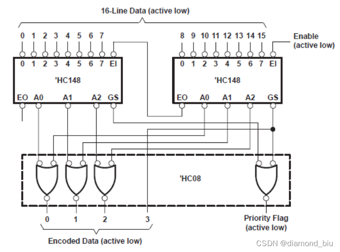
真值表如下:
`timescale 1ns/1ns
module encoder_83(input      [7:0]       I   ,input                  EI  ,output wire [2:0]      Y   ,output wire            GS  ,output wire            EO
);
assign {Y,GS,EO}=(~EI)?5'b00000:I[7]?5'b11110:I[6]?5'b11010:I[5]?5'b10110:I[4]?5'b10010:I[3]?5'b01110:I[2]?5'b01010:I[1]?5'b00110:I[0]?5'b00010:5'b00001;
endmodulemodule encoder_164(input      [15:0]      A   ,input                  EI  ,output wire [3:0]      L   ,output wire            GS  ,output wire            EO
);
wire GS1,GS2,EO1;
wire[2:0] L1,L2;
encoder_83 U1(.I(A[15:8]),.EI(EI),.Y(L1[2:0]),.GS(GS1),.EO(EO1));
encoder_83 U2(.I(A[7:0]),.EI(EO1),.Y(L2[2:0]),.GS(GS2),.EO(EO));
assign L={GS1,L1|L2};
assign GS=GS1|GS2;
endmodule
VL17 用3-8译码器实现全减器
全减器真值表如下,可以看到对于A B Ci来说,从上到下一次为最小项m0~m7,因此D=m1+m2+m4+m7,Co=m1+m2+m3+m7。将A B Ci接入题中3-8译码器,译码器输出Yi对应的是mi取反。
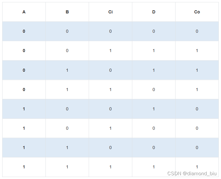
`timescale 1ns/1nsmodule decoder_38(input             E1_n   ,input             E2_n   ,input             E3     ,input             A0     ,input             A1     ,input             A2     ,output wire       Y0_n   ,  output wire       Y1_n   , output wire       Y2_n   , output wire       Y3_n   , output wire       Y4_n   , output wire       Y5_n   , output wire       Y6_n   , output wire       Y7_n
);
wire E ;
assign E = E3 & ~E2_n & ~E1_n;
assign  Y0_n = ~(E & ~A2 & ~A1 & ~A0);
assign  Y1_n = ~(E & ~A2 & ~A1 &  A0);
assign  Y2_n = ~(E & ~A2 &  A1 & ~A0);
assign  Y3_n = ~(E & ~A2 &  A1 &  A0);
assign  Y4_n = ~(E &  A2 & ~A1 & ~A0);
assign  Y5_n = ~(E &  A2 & ~A1 &  A0);
assign  Y6_n = ~(E &  A2 &  A1 & ~A0);
assign  Y7_n = ~(E &  A2 &  A1 &  A0);
endmodulemodule decoder1(input             A     ,input             B     ,input             Ci    ,output wire       D     ,output wire       Co
);
wire E3=1,E2_n=0,E1_n=0;
wire m0,m1,m2,m3,m4,m5,m6,m7;
decoder_38 U1(.E1_n(E1_n),.E2_n(E2_n),.E3(E3),.A0(Ci),.A1(B),.A2(A),.Y0_n(m0),.Y1_n(m1),.Y2_n(m2),.Y3_n(m3),.Y4_n(m4),.Y5_n(m5),.Y6_n(m6),.Y7_n(m7));
assign D=(~m1)|(~m2)|(~m4)|(~m7);
assign Co=(~m1)|(~m2)|(~m3)|(~m7);
endmodule
VL19 使用3-8译码器①实现逻辑函数
L=m1+m3+m6+m7,又因为3-8译码器的输出恰好是最小项取反,以ABC=111为例,对应最小项m7=1,对应译码器输出为Y7=0,因此只需要将译码器输出取反即为对应的最小项的值。

要点2:题目中表达式的最大项表达式为L=M0+M3+M4+M5,其中M0=A+B+C。最大项表式可以由最小项表示推导出。//module decoder_38省略,题目中直接给出了
module decoder0(input A ,input B ,input C ,output wire L
);wire E3=1,E2_n=0,E1_n=0;
wire m0,m1,m2,m3,m4,m5,m6,m7;
decoder_38 U1(.E1_n(E1_n),.E2_n(E2_n),.E3(E3),.A0(C),.A1(B),.A2(A),.Y0_n(m0),.Y1_n(m1),.Y2_n(m2),.Y3_n(m3),.Y4_n(m4),.Y5_n(m5),.Y6_n(m6),.Y7_n(m7));assign L=(~m1)|(~m3)|(~m6)|(~m7);endmodule
VL20 数据选择器实现逻辑电路
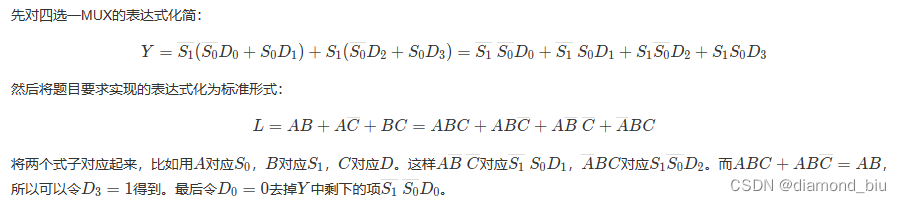
`timescale 1ns/1ns
module data_sel(input             S0     ,input             S1     ,input             D0     ,input             D1     ,input             D2     ,input             D3     ,output wire        Y
);assign Y = ~S1 & (~S0&D0 | S0&D1) | S1&(~S0&D2 | S0&D3);
endmodulemodule sel_exp(input             A     ,input             B     ,input             C     ,output wire       L
);
data_sel U1(.S0(A),.S1(B),.D0(0),.D1(~C),.D2(C),.D3(1),.Y(L));
endmodule
VL21 根据状态转移表实现时序电路
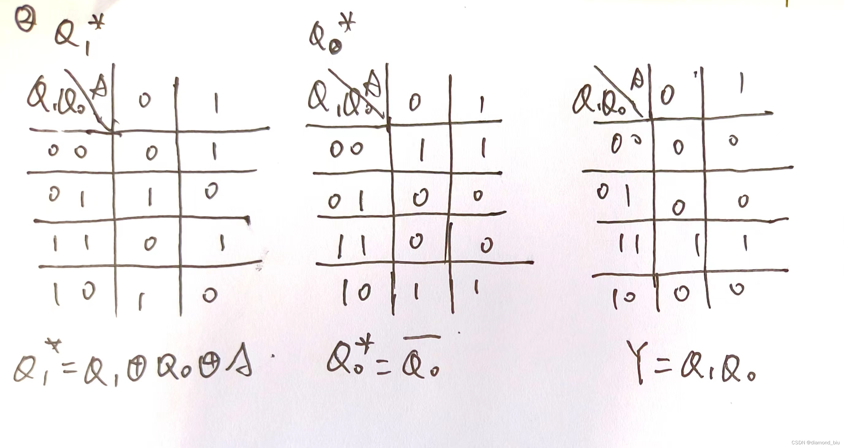
`timescale 1ns/1nsmodule seq_circuit(input                A   ,input                clk ,input                rst_n,output   wire        Y
);
reg Q1,Q0;
always @ (posedge clk or negedge rst_n) beginif(!rst_n) beginQ1<=0;Q0<=0;endelse beginQ1<=Q1^Q0^A;Q0<=~Q0;end
end
assign Y=Q1&Q0;
endmodule
经典三段式`timescale 1ns/1nsmodule seq_circuit(input A ,input clk ,input rst_n,output reg Y
);reg[1:0] current_state,next_state;
always @ (posedge clk or negedge rst_n) beginif(!rst_n) current_state<=2'b00;else current_state<=next_state;
end
always @ (current_state or A) beginnext_state<=2'b00;case(current_state)2'b00:beginif(A)next_state<=2'b11;else next_state<=2'b01;end2'b01:beginif(A)next_state<=2'b00;else next_state<=2'b10;end2'b10:beginif(A)next_state<=2'b01;else next_state<=2'b11;end2'b11:beginif(A)next_state<=2'b10;else next_state<=2'b00;endendcase
end
always @ (*) begincase(current_state)2'b00:beginif(A)Y<=0;else Y<=0;end2'b01:beginif(A)Y<=0;else Y<=0;end2'b10:beginif(A)Y<=0;else Y<=0;end2'b11:beginif(A)Y<=1;else Y<=1;endendcase
endendmodule
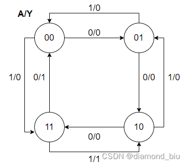
VL22 根据状态转移图实现时序电路
要点1:同步时序电路设计流程,需要注意的是Y需要写成组合逻辑。
`timescale 1ns/1nsmodule seq_circuit(input                C   ,input                clk ,input                rst_n,output   wire        Y
);
reg Q1,Q0;
always @ (posedge clk or negedge rst_n) beginif(!rst_n) beginQ0<=0;Q1<=0;endelse beginQ1<=(Q0&(~C))|(Q1&C);Q0<=(Q0&(~C))|((~Q1)&C);end
end
assign Y=(Q1&Q0)|(Q1&C);
endmodule
`timescale 1ns/1nsmodule seq_circuit(input                C   ,input                clk ,input                rst_n,output   reg        Y
);
reg[1:0] current_state,next_state;
always @ (posedge clk or negedge rst_n) beginif(!rst_n) current_state<=2'b00;else current_state<=next_state;
end
always @ (current_state or C) beginnext_state<=2'b00;case(current_state)2'b00:beginif(C)next_state<=2'b01;else next_state<=2'b00;end2'b01:beginif(C)next_state<=2'b01;else next_state<=2'b11;end2'b10:beginif(C)next_state<=2'b10;else next_state<=2'b00;end2'b11:beginif(C)next_state<=2'b10;else next_state<=2'b11;endendcase
end
always @ (*) begincase(current_state)2'b00:beginif(C)Y<=0;else Y<=0;end2'b01:beginif(C)Y<=0;else Y<=0;end2'b10:beginif(C)Y<=1;else Y<=0;end2'b11:beginif(C)Y<=1;else Y<=1;endendcase
end
endmodule
VL23 ROM的简单实现
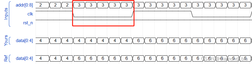
//这种写法不正确
/*
`timescale 1ns/1ns
module rom(input clk,input rst_n,input [7:0]addr,output reg[3:0]data
);
reg[0:3] rom_array [7:0];
always @ (posedge clk or negedge rst_n) beginif(!rst_n) beginrom_array[0]<=4'd0;rom_array[1]<=4'd2;rom_array[2]<=4'd4;rom_array[3]<=4'd6;rom_array[4]<=4'd8;rom_array[5]<=4'd10;rom_array[6]<=4'd12;rom_array[7]<=4'd14;data<=0;endelse begindata<=rom_array[addr];end
end
endmodule
*/
`timescale 1ns/1ns
module rom(input clk,input rst_n,input [7:0]addr,output [3:0]data
);reg[0:3] rom_array [7:0];always @ (posedge clk or negedge rst_n) beginif(!rst_n) beginrom_array[0]<=4'd0;rom_array[1]<=4'd2;rom_array[2]<=4'd4;rom_array[3]<=4'd6;rom_array[4]<=4'd8;rom_array[5]<=4'd10;rom_array[6]<=4'd12;rom_array[7]<=4'd14;endelse ;
end
assign data=rom_array[addr];
endmodule
VL24 边沿检测
a[0]&(~a[1]),下降沿检测即(~a[0])&a[1]。
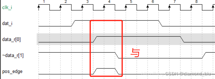
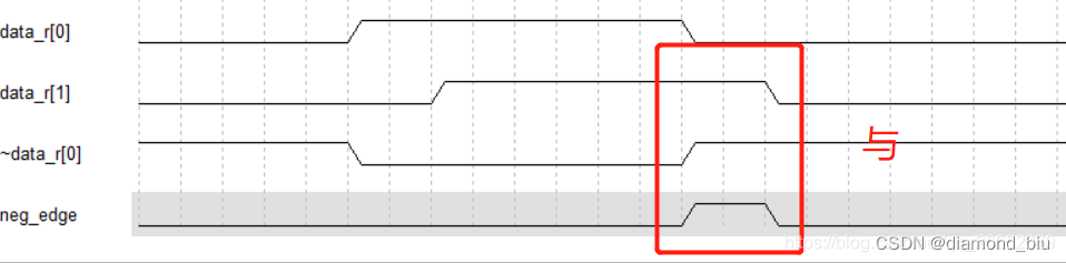
图中边沿检测多延迟了一拍。
本题用a0存储a的上一个状态,01((~a0)&a)即为上升沿,10即为下降沿(a0(~a)),其余情况既不是上升沿也不是下降沿。`timescale 1ns/1ns
module edge_detect(input clk,input rst_n,input a,output reg rise,output reg down
);
reg a0;
always @ (posedge clk or negedge rst_n) beginif(!rst_n) beginrise<=0;down<=0;endelse begina0<=a;if(a&(~a0))rise<=1;else if((~a)&a0)down<=1;else beginrise<=0;down<=0;endend
endendmodule
{reg_a,a}改变时发生状态转移。(这是sh的写法`timescale 1ns/1ns
module edge_detect(input clk,input rst_n,input a,output reg rise,output reg down
);reg [1:0]current_state;
reg [1:0]next_state;
reg reg_a;always @(posedge clk or negedge rst_n) beginif (!rst_n) current_state <= 0;else current_state <= next_state;
endalways @(*) begincase (current_state)2'b00:beginrise = 0;down = 0;end2'b01:beginrise = 1;down = 0;end2'b10:beginrise = 0;down = 1;end2'b11:beginrise = 0;down = 0;endendcase
endalways @(posedge clk or negedge rst_n)beginif (!rst_n) reg_a <= 0;else reg_a <= a;
endalways @(a or reg_a) begincase ({reg_a,a})2'b00:next_state = 2'b00;2'b01:next_state = 2'b01;2'b10:next_state = 2'b10;2'b11:next_state = 2'b00;endcase
endendmodule
current_state和next_state的初始状态要设置为11,但是由于这是查看错误样例后才知道的,因此需要添加的idle作为初始无效状态,当检测到有效信号后再进入对应状态,0则进入00状态,1则进入11状态。if(a==1)...;else...;本意是a为1和0时分别跳转到下一个状态,但由于所给测试向量存在无效状态,因此条件判断改为了if(a==1)...;else if(a==0)...;else next_state=idle;这样就可以在出现无效状态时不产生异常的状态跳转。case(next_state),如果写成组合逻辑为case(current_state),两种写法在下示代码都有显示。`timescale 1ns/1ns
module edge_detect(input clk,input rst_n,input a,output reg rise,output reg down
);parameter idle=3'b111;reg[2:0] current_state,next_state;always @ (posedge clk or negedge rst_n) beginif(!rst_n)current_state<=idle;else current_state<=next_state;endalways @ (current_state or a) beginnext_state=idle;case(current_state)3'b000:beginif(a==1)next_state=3'b001;else if(a==0)next_state=3'b000;else next_state=idle;end3'b001:beginif(a==1)next_state=3'b011;else if(a==0) next_state=3'b010;else next_state=idle;end3'b010:beginif(a==1)next_state=32'b001;else if(a==0)next_state=3'b000;else next_state=idle;end3'b011:beginif(a==1)next_state=3'b011;else if(a==0)next_state=3'b010;else next_state=idle;endidle:beginif(a==1)next_state=3'b011;else if(a==0)next_state=3'b000;else next_state=idle;enddefault:next_state=idle;endcaseendalways@(*)begincase(current_state)3'b000:begin rise=0;down=0;end3'b001:begin rise=1;down=0;end3'b010:begin rise=0;down=1; end3'b011:begin rise=0;down=0; end3'b111:begin rise=0;down=0;enddefault:begin rise=0;down=0; endendcaseend/*always @(posedge clk or negedge rst_n)beginif(~rst_n)beginrise<=0;down<=0;endelse begincase(next_state)3'b000:begin rise<=0;down<=0;end3'b001:begin rise<=1;down<=0;end3'b010:begin rise<=0;down<=1; end3'b011:begin rise<=0;down<=0; end3'b111:begin rise<=0;down<=0;enddefault:begin rise<=0;down<=0; endendcaseendend
*/
endmodule
Verilog进阶挑战
Verilog企业真题
VL25 输入序列连续的序列检测
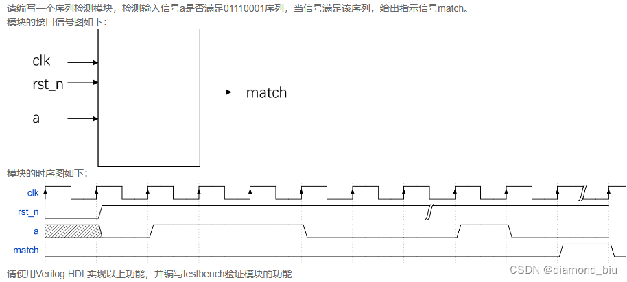
s0:初始状态,没有匹配到任何序列;
s1:匹配到序列'0';
…
s8:匹配到序列'01110001';
需要的注意的状态跳转遇到不匹配时并不是直接跳转回s0,应该跳转回最长匹配子序列对应的状态。`timescale 1ns/1ns
module sequence_detect(input clk,input rst_n,input a,output reg match);parameter s0=4'd0,s1=4'd1,s2=4'd2,s3=4'd3,s4=4'd4,s5=4'd5,s6=4'd6,s7=4'd7,s8=4'd8;reg[3:0] current_state,next_state;always @ (posedge clk or negedge rst_n) beginif(~rst_n) current_state<=s0;else current_state<=next_state;endalways @ (a,current_state)beginnext_state=s0;case(current_state)s0:next_state=a?s0:s1;s1:next_state=a?s2:s1;s2:next_state=a?s3:s1;s3:next_state=a?s4:s1;s4:next_state=a?s0:s5;s5:next_state=a?s2:s6;s6:next_state=a?s2:s7;s7:next_state=a?s8:s1;s8:next_state=a?s3:s1;default:next_state=s0;endcaseendalways @ (posedge clk or negedge rst_n) beginif(!rst_n) match<=0;else begincase(current_state)s8:match<=1;default:match<=0;endcaseendendendmodule
`timescale 1ns/1ns
module sequence_detect(input clk,input rst_n,input a,output reg match);reg[7:0] q;always @ (posedge clk or negedge rst_n) beginif(!rst_n) beginq<=8'b0;endelse beginq<={q[6:0],a};endendalways @ (posedge clk or negedge rst_n) beginif(!rst_n) beginmatch<=0;endelse beginif(q==8'b01110001)match<=1;else match<=0;endend
endmodule
VL38 自动贩售机1
`timescale 1ns/1ns
module seller1(input wire clk  ,input wire rst  ,input wire d1 ,input wire d2 ,input wire d3 ,output reg out1,output reg [1:0]out2
);
//*************code***********//
reg [2:0] current_state,next_state;always @ (posedge clk or negedge rst) beginif(!rst) begin current_state<=3'b000;endelse current_state<=next_state;
endalways@(current_state or d1 or d2 or d3)beginnext_state<=3'b000;case(current_state)3'b000:beginif ({d3,d2,d1}==3'b001) next_state=3'b001;else if({d3,d2,d1}==3'b010) next_state=3'b010;else if({d3,d2,d1}==3'b100) next_state=3'b100;else next_state=3'b000;end3'b001:beginif ({d3,d2,d1}==3'b001) next_state=3'b010;else if({d3,d2,d1}==3'b010) next_state=3'b011;else if({d3,d2,d1}==3'b100) next_state=3'b101;else next_state=3'b001;end3'b010:beginif ({d3,d2,d1}==3'b001) next_state=3'b011;else if({d3,d2,d1}==3'b010) next_state=3'b100;else if({d3,d2,d1}==3'b100) next_state=3'b110;else next_state=3'b010;end3'b011:beginif ({d3,d2,d1}==3'b001) next_state=3'b001;else if({d3,d2,d1}==3'b010) next_state=3'b010;else if({d3,d2,d1}==3'b100) next_state=3'b100;else next_state=3'b000;end3'b100:beginif ({d3,d2,d1}==3'b001) next_state=3'b001;else if({d3,d2,d1}==3'b010) next_state=3'b010;else if({d3,d2,d1}==3'b100) next_state=3'b100;else next_state=3'b000;end3'b101:beginif ({d3,d2,d1}==3'b001) next_state=3'b001;else if({d3,d2,d1}==3'b010) next_state=3'b010;else if({d3,d2,d1}==3'b100) next_state=3'b100;else next_state=3'b000;end3'b011:beginif ({d3,d2,d1}==3'b001) next_state=3'b001;else if({d3,d2,d1}==3'b010) next_state=3'b010;else if({d3,d2,d1}==3'b100) next_state=3'b100;else next_state=3'b000;enddefault:next_state=3'b000;endcase
end
always @ (posedge clk or negedge rst) beginif(!rst) beginout1<=0;out2<=0;endelse begincase(next_state)3'b000:begin out1<=1'd0;out2<=2'd0; end3'b001:begin out1<=1'd0;out2<=2'd0; end3'b010:begin out1<=1'd0;out2<=2'd0; end3'b011:begin out1<=1'd1;out2<=2'd0; end3'b100:begin out1<=1'd1;out2<=2'd1; end3'b101:begin out1<=1'd1;out2<=2'd2; end3'b110:begin out1<=1'd1;out2<=2'd3; enddefault:begin out1<=1'd0;out2<=2'd0; endendcaseend
end
//*************code***********//
endmodule
常见数字IC手撕代码